A reading companion to the complete German service manual, schematic and both board layouts. This is our own technical guide, translated between German, English and Russian; it is not a complete translation of the historical manual.
Which power supply does this cover?
Reference circuit: 56-330-2770-5. PSU001/PSU002 identifications below use photographs and placement drawing 63-330-2760-4. They are layout correlations, not continuity tests. The installed museum W/M supply has not been matched; factory population and replacement suitability remain unverified.
Specimens and restoration scope
Owner-reported inventory and intended use. The additional vertical PCB is absent from both PSU001 and PSU002; its exact assembly revision is not yet identified.
| Specimen | Shield identification | Condition / intended use |
|---|---|---|
| PSU001 | — | Vertical PCB missing; retained for parts or possible custom PSU installation. |
| PSU002 | 043024 | Vertical PCB and V15 transistor missing; retained for parts or possible custom PSU installation. |
| PSU003 | S/N 010438 | Current restoration focus. Completeness and electrical condition not yet assessed. |
PSU002 photographs
PSU002 is a separate assembly, reported by the owner as otherwise identical to PSU001. Its V15 mounting position is empty; see the comparison below. Owner-reported shield number: 043024; no serial-number stamp observed on the PCB.
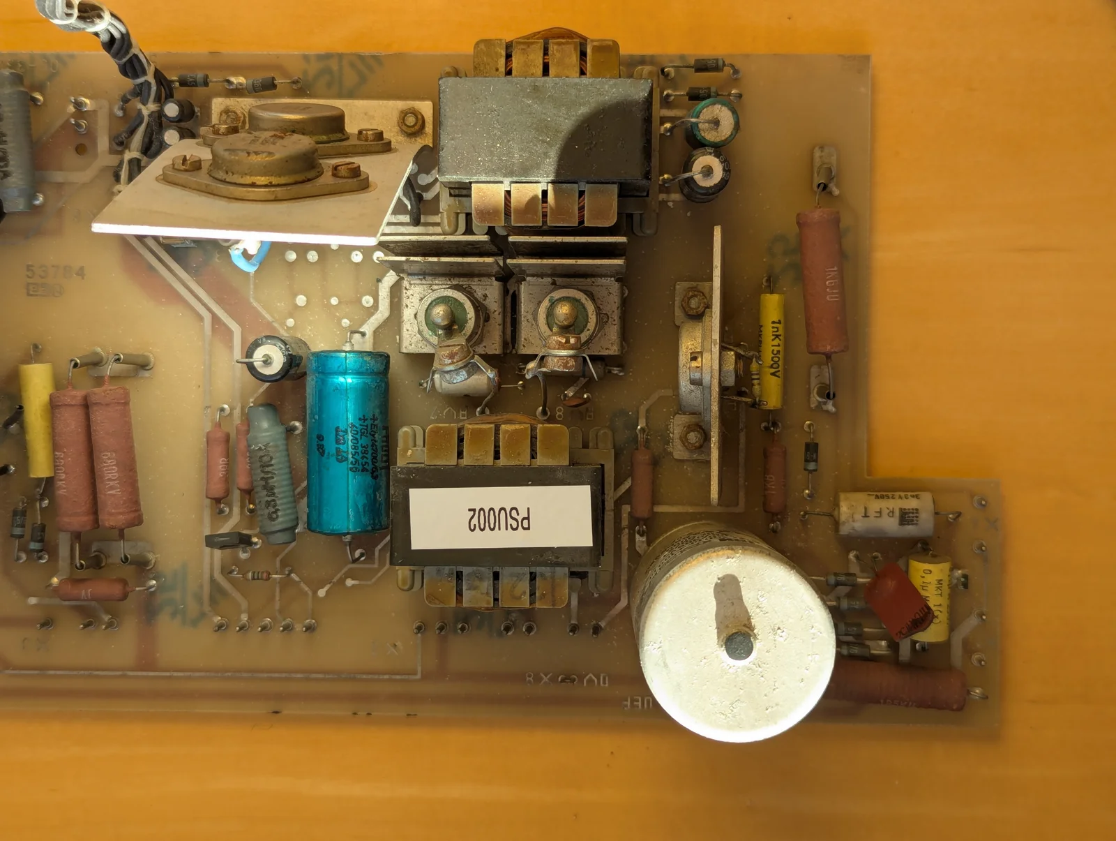
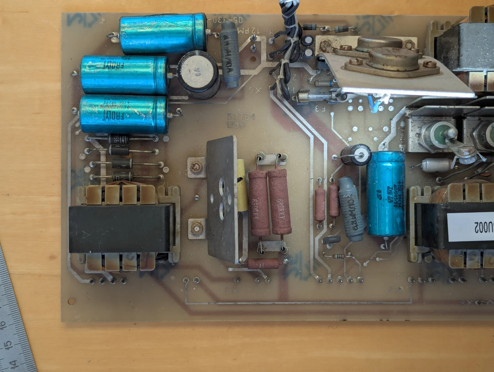
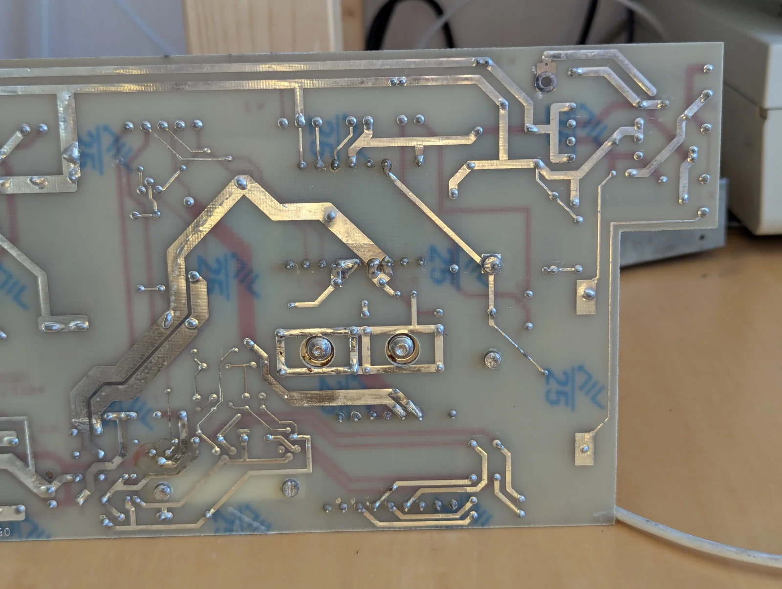
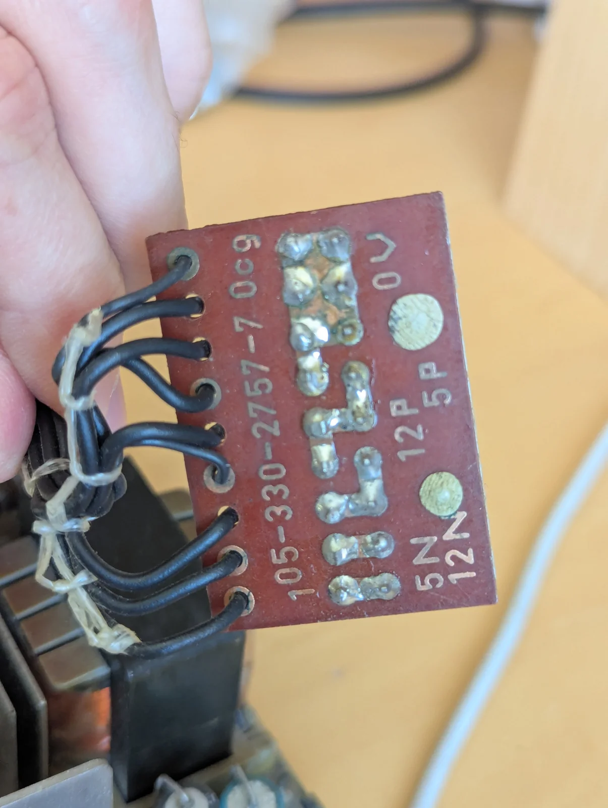
Original photographs and provenance · Danila · 2026-10-19
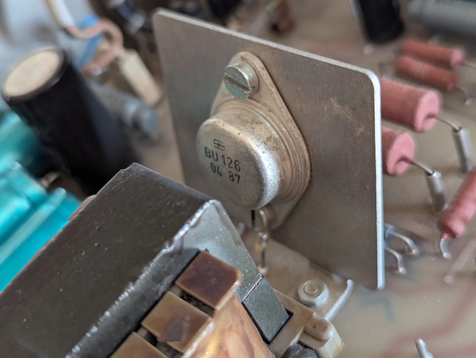
PSU001: the fitted BU126
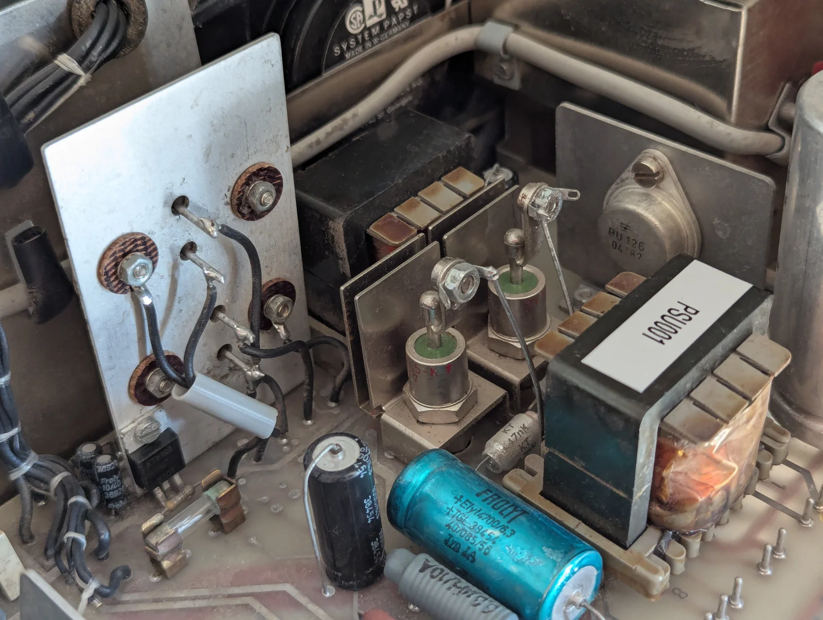
The PSU001 transistor is marked BU126 / 04 87. Its heatsink and surrounding parts match V15 in the placement drawing.
PSU001 originals and provenance · Danila · 2026-10-19
Board locator and specimen comparison
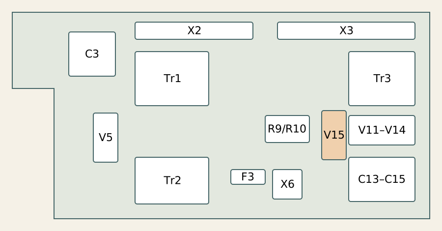
F3 is the fuse in the switched 12P path; X6 serves the monitor output. R120, R130 and R160 are on the separate control board: use its placement drawing (PDF 19) and the reference checks.
| Position | Reference drawing | Photographed specimens |
|---|---|---|
| V15 | SU169; primary switch for Tr3 / 12PM | PSU001: BU126; PSU002: empty. Position matched by R9/R10, Tr3, V11–V14 and C13–C15. |
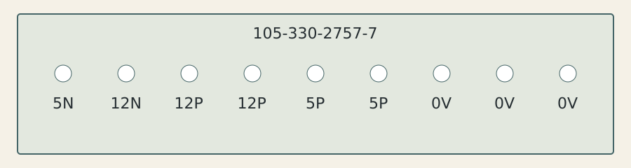
| XNT rail groups | 5N; 12N; 12P ×2; 5P ×2; 0V ×3 | Connector PCB 105-330-2757-7: labels and solder bridges agree with these groups. |
Read the German originals
Full documents open at their original hosts. Page numbers below refer to the specific scans in the source register. These archives retain their credits and rights; they are not included in the museum’s MIT licence.
- Complete service manual · PSU chapter
- Complete schematic collection · PSU circuit
- Power board layout
- Control board layout
- 1715 / 1715W operating manual
- W/M archive · comparison material
| Topic | Printed page | PDF page |
|---|---|---|
| Overview, construction, mains input | 93 | 95 |
| Startup and 5P converter | 94 | 96 |
| 5P regulation and protection | 95 | 97 |
| Negative rails and 12PM converter | 96 | 98 |
| 12PM control and 12P switching | 97 | 99 |
| Sequencing and overvoltage protection | 98 | 100 |
| Original block diagram | 99 | 101 |
| Adjustment procedure, first page | 100 | 102 |
| Adjustment procedure, continuation | 101 | 103 |
Rails and connector names
Keep the net labels unchanged in every language. “P” denotes a positive rail, “N” a negative rail. 12PM is the monitor supply; 12P is its separately switched output. The primary return is not the secondary 0 V.
| Net | Reference function | Connector / value |
|---|---|---|
| 5P | Logic supply | XNT 5, 6 · +5 V |
| 12PM | Monitor supply before V18 | X MONU 2 / X6 3 · +12 V |
| 12P | Switched drive supply after V18 and F3 | XNT 3, 4 · +12 V |
| 5N | Negative supply | XNT 1 · −5 V |
| 12N | Negative supply | XNT 2 · −12 V |
| 0 V | Secondary return | XNT 7, 8, 9; X MONU 1 / X6 2 |
These are schematic pin numbers, not a mating-face drawing. Confirm connector orientation by tracing a disconnected assembly. The monitor connector’s third contact is shown as protective earth/shield; do not treat it as an interchangeable load return. Connector names can recur elsewhere in the computer.
Connector orientation
Solder side, with the 105-330-2757-7 printing upright: left to right, the pad groups are shown below. This drawing follows the labelled connector photo. It does not number the mating face: pin 1 there still requires a confirmed correspondence to these pads.
How to read the circuit
Read the power paths and the feedback paths separately. V5 and V15 are primary switching transistors; V18 is a secondary PNP series switch. A modern transistor suitable for V18 therefore says nothing about suitability at V5. The 5P section is a forward converter; the 12PM section is a flyback converter. Negative outputs depend on loading of 5P. The 12P delay belongs to the real supply, not the emulator’s power animation.
Reference values and interpretation
The following are reference checks, not an instruction to adjust an unidentified or faulty unit. The original procedure supplies the complete loading conditions and order. Mains-side measurements and repairs require appropriate isolation, probes and trained handling; C3 can retain hazardous voltage after unplugging. An earthed oscilloscope ground must not be attached to the primary return.
| Item | Documented value / condition | Where |
|---|---|---|
| Mains input | 220 V; 47–63 Hz; 187–242 V | §1.9.3 · 93 / PDF 95 |
| 5P setting | 5.10 V ±50 mV; R130; I(5P)=5 A; R(5N)=10 Ω; R(12N)=56 Ω | §1.9.9.1 · 100 / PDF 102 |
| Negative-rail validity | I(5P) ≥1.5 A | §1.9.7 · 96 / PDF 98 |
| 12PM setting | 12.2 V ±100 mV; R160; I(5P)=5 A; I(12P)=3 A; X6 / DISPLAY | §1.9.9.4 · 100 / PDF 102 |
| 12P sequencing | 2.0–4.5 s; 5P, 5N, 12N, 12PM → 12P | §1.9.9.7 · 101 / PDF 103 |
| 12P mains-failure threshold | UEP 195 V → 12P OFF; UEP 200 V → 12P ON; R120 | §1.9.9.6 · 101 / PDF 103 |
A reading of about 12 V on DISPLAY does not prove that 12P is present. Conversely, missing 12P does not by itself prove V18 failed: F3, the drive stage, undervoltage detection and delay circuitry are distinct possibilities. Inspect them as separate hypotheses. Do not bridge F3 or V18 to make the symptom disappear. A no-load reading on a negative rail cannot establish a regulator fault.
Transistors in the reference drawing
| Reference | Marked type | Circuit role |
|---|---|---|
| V5, V15 | SU169 | Primary power switches |
| V18 | КТ818А / KT818A | 12P series switch |
| V19 | SD336B | V18 drive |
| V101, V102 | SF358 | Startup cascade |
| V106 | SD335B | Auxiliary regulator |
| V107, V125 | SC236D | Auxiliary control / 12P control |
| V110, V119 | SF127C | Pulse-transformer drivers |
The list covers the discrete transistor symbols in this drawing, not every semiconductor. U101–U105 are optocouplers; the drawing also contains diodes and regulator/control ICs. The PCB layouts can differ in populated details from this circuit sheet: match revisions rather than silently merging them into one bill of materials.
Soviet and modern replacement candidates
No substitution below has been tested in this museum PSU. “Candidate” means worth evaluating in the identified circuit, not a verified repair or a pin-compatible equivalent. The most defensible starting point is V18, because the reference itself already specifies the Soviet КТ818А.
| Position / candidate | Evidence | Decision and remaining checks |
|---|---|---|
| V18 · КТ818Б (KT818B) | Same Soviet type family. INTEGRAL specifies 10 A, 60 W at case ≤25 °C, and h21э ≥20 for Б versus ≥15 for А at its stated test point. [kt818] | A strong family candidate, subject to the exact maker/package datasheet, authenticity and condition. Verify saturation at the available base drive, mounting and switch-off timing. The Cyrillic Б is transliterated B; Cyrillic В is V. Do not confuse the grades. |
| V18 · ST TIP36C | PNP; |VCEO| 100 V, |IC| 25 A, 125 W at case 25 °C; TO-247. ST lists the part active. [tip36] [tip36-status] | Modern candidate requiring a mounting/wiring review. INTEGRAL КТ818 uses 1=E, 2=C, 3=B; TIP36C uses 1=B, 2=C, 3=E. Do not fit it by matching pin positions. Absolute ratings do not prove adequate gain, safe operating area or low voltage drop at 3–5 A in this driver. |
| V5 / V15 · onsemi FJL6920 | NPN; VCEO 800 V, IC 20 A, 200 W at case 25 °C; TO-264. Gain at 11 A is only 5.5–8.5; saturation is specified with 2.75 A base drive. [fjl] | Comparison example only; NOT approved as an SU169 replacement. Its larger headline ratings do not establish compatibility with Tr101/Tr102. Storage time, reverse base drive, safe operating area and mounting need circuit-specific validation. No Soviet or modern replacement is qualified here for these primary switches. |
For SF358, SD335B, SD336B, SC236D and SF127C, this edition deliberately leaves the replacement open until original manufacturer data and the actual circuit stresses are compared. A cross-reference search result is not enough. Retain gain-group suffixes. A MOSFET or Darlington is not a direct substitute for an ordinary bipolar transistor in this circuit.
What would make a substitution verified?
Record the actual PSU assembly/revision, removed part marking, replacement manufacturer and lot, lead-to-net mapping and insulation. Verify turn-on and turn-off sequencing, saturation drop, dissipation and temperature over the specified loads and mains range. Check startup, transient load and protection behaviour with suitable test equipment. For primary switches, include collector and base waveforms and safe-operating-area margins. Attach measured results before changing a candidate to “bench-qualified”. No such measurements were made for this publication.
Translation glossary
| German | English | Русский |
|---|---|---|
| Stromversorgung / Netzteil | power supply / PSU | блок питания / БП |
| Durchflusswandler | forward converter | прямоходовой преобразователь |
| Sperrwandler | flyback converter | обратноходовой преобразователь |
| Freilaufdiode | freewheel diode | диод свободного хода |
| Anlaufschaltung | startup circuit | цепь запуска |
| Langsamanlauf | soft start | плавный пуск |
| Aussetzerbetrieb | intermittent operation | прерывистый режим |
| Schmelzsicherung | fuse | плавкий предохранитель |
| Uss | peak-to-peak voltage | напряжение от пика до пика |
| B / C / E | base / collector / emitter | база / коллектор / эмиттер |
Verification and unresolved points
The schematic, both placement drawings and the service check pages were inspected as images; OCR was used only as a navigation aid. Numerical tables are shared across the three editions. The guide preserves the distinction between printed and PDF page numbers. The service text at §1.9.8.1 refers to V12 as a power switch, whereas the circuit identifies V15 and places V12 among the rectifier diodes: use the drawing to resolve that discrepancy. Translation and source review were performed in one editorial pass; there has been no independent human technical review or hardware validation.
Sources and credits
Original engineering: Robotron. Preservation hosts and component manufacturers are credited below. Museum commentary and translations: DAC / Danila, AI-assisted, 2026-10-19. Linked documents retain their own rights. Source checksums and access records are available in the machine-readable register.
-
Robotron · 1715 Servicehandbuch
VEB Robotron Büromaschinenwerk Sömmerda; archive: tiffe.de
§1.9; 93–101 → PDF 95–103 -
Robotron · Schaltpläne
Robotron; archive: tiffe.de
56-330-2770-5; PDF 18–20 -
Robotron · Bedienungsanleitung 1715 / 1715W
Robotron; digitisation: Ulrich Zander; mirror: XEPb.org
1715 / 1715W -
Robotron 1715 unofficial support
XEPb.org / DtZ; links credit Ulrich Zander and Jens Müller
1715W archive: https://xepb.org/robotron/docs/1715w.zip -
КТ818 · January 2011, rev. 1.0
ОАО «ИНТЕГРАЛ», Minsk; mirror: Arbatex
PDF 1–3; аАО.336.188 ТУ / 02 -
TIP35C / TIP36C · September 2008, rev. 5
STMicroelectronics
PDF 1–3, 7; TIP36C is the PNP member -
TIP36C · product status
STMicroelectronics
Active; checked 2026-10-19 -
FJL6920 · January 2025, rev. 2
onsemi
PDF 1–2; comparison only